The fab table for 2026 serves as a critical strategic roadmap for the semiconductor industry, detailing projected wafer capacities, technology node transitions, and capital expenditure trends across global foundries. As the market shifts toward advanced packaging and specialized process nodes, understanding these metrics is essential for supply chain planning. This guide analyzes the latest pricing dynamics, compares top manufacturing models from leaders like TSMC, Samsung, and Intel, and highlights the technological pivots defining the next era of chip production.
What Is a Fab Table and Why It Matters in 2026
A fab table is not merely a spreadsheet; it is a comprehensive dataset representing the operational heartbeat of the global semiconductor ecosystem. In 2026, this data has evolved to include granular details on heterogeneous integration, power efficiency metrics, and regional supply resilience. Industry analysts rely on these tables to forecast availability for high-performance computing (HPC) and automotive sectors.
The significance of the fab table has grown due to geopolitical shifts and the explosion of AI-driven demand. Unlike previous years where capacity was the sole metric, the 2026 landscape prioritizes technology readiness and yield stability. Companies use this data to mitigate risks associated with single-source dependencies and to align product roadmaps with foundry capabilities.
Furthermore, the modern fab table integrates sustainability benchmarks. With strict carbon regulations coming into force, manufacturers now list energy consumption per wafer and water recycling rates alongside traditional throughput numbers. This holistic view allows stakeholders to make decisions that balance performance with environmental compliance.
Key Technology Trends Shaping the 2026 Fabrication Landscape
The semiconductor fabrication sector in 2026 is defined by three dominant forces: the maturation of Gate-All-Around (GAA) transistors, the rise of backside power delivery, and the ubiquity of chiplet-based architectures. These trends are reshaping how the fab table is structured and interpreted by engineers and procurement officers alike.
The Dominance of GAA and Nanosheet Architectures
By 2026, FinFET technology has largely reached its physical limits for leading-edge nodes. The industry has widely adopted Gate-All-Around (GAA) structures, often referred to as nanosheets. This transition offers superior electrostatic control, allowing for continued scaling without excessive leakage.
- Improved Performance: GAA provides up to 15% better performance at the same power level compared to final-generation FinFETs.
- Design Flexibility: Foundries can adjust the width of nanosheets to tune drive current, offering more customization for specific workloads.
- Scaling Continuity: This architecture supports scaling down to the 18A and 14A equivalents, ensuring a clear path for future density improvements.
Manufacturers updating their fab table entries now explicitly denote GAA readiness as a primary differentiator. Clients seeking maximum efficiency for mobile SoCs or data center GPUs prioritize facilities equipped with these advanced lithography tools.
Backside Power Delivery Networks (BSPDN)
Another revolutionary shift visible in the 2026 fab table is the implementation of Backside Power Delivery Networks. Traditionally, power and signal wires competed for space on the front side of the silicon. BSPDN moves power routing to the rear of the wafer.
This architectural change yields significant benefits. It reduces IR drop, improves signal integrity, and frees up valuable real estate on the front side for logic transistors. Leading foundries have begun volume production using this technique, marking a pivotal moment in Moore’s Law evolution. Designers must now account for new design rules when selecting a fabrication partner.
Advanced Packaging and Chiplet Integration
The definition of a “fab” has expanded beyond front-end manufacturing. In 2026, the fab table increasingly includes backend-of-line (BEOL) capabilities, specifically advanced packaging services like 2.5D and 3D integration. The era of monolithic chips is giving way to modular designs.
Chiplets allow manufacturers to mix and match process nodes. A high-speed compute die might be fabricated on a 3nm node, while I/O and memory components use mature, cost-effective nodes. This strategy optimizes yield and reduces overall system costs. Foundries offering seamless integration between front-end logic and back-end packaging are seeing the highest demand.
2026 Fab Table Comparison: Top Models and Foundries
To navigate the complex supplier landscape, we have compiled a comparative analysis of the leading fabrication models available in 2026. This fab table comparison highlights key differentiators in node naming, packaging technologies, and target applications.
| Foundry Model |
Leading Node (2026) |
Key Architecture |
Packaging Tech |
Primary Focus |
| TSMC N2 Series |
2nm (N2P) |
GAA Nanosheet |
CoWoS-L / SoIC |
AI Accelerators, Mobile |
| Samsung SF2 |
2nm (SF2LPP) |
GAA MBCFET |
I-CubeX |
HPC, Automotive |
| Intel 18A |
18 Angstrom |
RibbonFET + BSPDN |
Foveros Direct |
Data Center, Client CPU |
| GlobalFoundries |
12LP+ / RF |
FinFET (Mature) |
2.5D Interposers |
IoT, Automotive, 5G |
| UMC |
22nm / 28nm |
Planar / FinFET |
Standard Bump |
Display Drivers, PMIC |
This fab table snapshot reveals a clear divergence in strategy. While TSMC and Samsung battle for the bleeding edge of logic density, Intel is leveraging its unique backside power technology to leapfrog competitors in power efficiency. Meanwhile, specialty foundries like GlobalFoundries and UMC dominate the mature node sector, which remains crucial for analog, RF, and power management integrated circuits (PMIC).
Pricing Dynamics and Cost Structures in 2026
Understanding the cost implications of the fab table is vital for budgeting and product viability. In 2026, wafer pricing has stabilized after the volatility of the early decade, but a distinct premium exists for leading-edge nodes. The cost per wafer is no longer just about lithography steps; it includes expensive metrology, defect inspection, and advanced packaging overheads.
Leading-Edge vs. Mature Node Economics
The price gap between 3nm-class nodes and mature 28nm processes has widened. A 300mm wafer at the 2nm node can cost significantly more than its predecessors due to the extreme complexity of EUV lithography layers. However, the transistor cost continues to decrease, making advanced nodes viable for a broader range of applications beyond just flagship smartphones.
- Mask Costs: Photomask sets for sub-3nm nodes remain a massive upfront investment, often exceeding tens of millions of dollars.
- Yield Learning: Early adopters pay a “risk premium.” As yields mature throughout 2026, effective costs per good die decrease substantially.
- Packaging Add-ons: Advanced packaging can add 20-30% to the total manufacturing cost but is often necessary to achieve system-level performance goals.
For companies analyzing the fab table for cost optimization, the strategy often involves right-sizing the node. Using a 5nm node for a component that only requires 7nm performance results in unnecessary expenditure. Conversely, under-specifying can lead to thermal throttling and poor user experience.
Regional Pricing Variations
Geopolitical factors have introduced regional pricing tiers. Subsidies from the CHIPS Act in the US and similar initiatives in Europe and Asia have altered the effective cost structure for local production. While base wafer prices remain globally competitive, the total landed cost now includes logistics security premiums and inventory buffering strategies.
Supply chain managers must look beyond the headline price in the fab table. They need to consider long-term supply agreements (LTSA), capacity reservation fees, and the potential for government incentives that can offset initial capital outlays. Flexibility in sourcing across different geographic regions is becoming a standard requirement for resilience.
Strategic Applications: Who Needs Which Fab Model?
Selecting the right entry from the fab table depends entirely on the application domain. There is no one-size-fits-all solution in 2026. Different industries prioritize different attributes, ranging from raw speed to long-term availability and temperature tolerance.
Artificial Intelligence and High-Performance Computing
For AI training clusters and inference engines, the priority is maximum transistor density and memory bandwidth. These applications demand the latest nodes (2nm/18A) coupled with advanced 2.5D or 3D packaging. The ability to integrate HBM (High Bandwidth Memory) directly adjacent to the logic die is non-negotiable.
Companies in this sector closely monitor the fab table for CoWoS and Foveros capacity allocations. Shortages in packaging slots often bottleneck production more than wafer fabrication itself. Securing capacity here requires multi-year commitments and close collaboration with foundry engineering teams.
Automotive and Industrial IoT
The automotive sector presents a different set of requirements. Reliability, longevity, and operation in harsh environments take precedence over cutting-edge speed. Consequently, the fab table entries for 40nm, 28nm, and 22nm FD-SOI nodes are highly relevant for this segment.
- Safety Certification: Processes must support ISO 26262 ASIL-D standards.
- Temperature Range: Chips must operate reliably from -40°C to 150°C.
- Supply Longevity: Automotive lifecycles span 10-15 years, requiring guaranteed process availability.
Specialty foundries excel here, offering robust analog mixed-signal capabilities embedded within mature digital flows. The focus is on minimizing field failures rather than maximizing clock speeds.
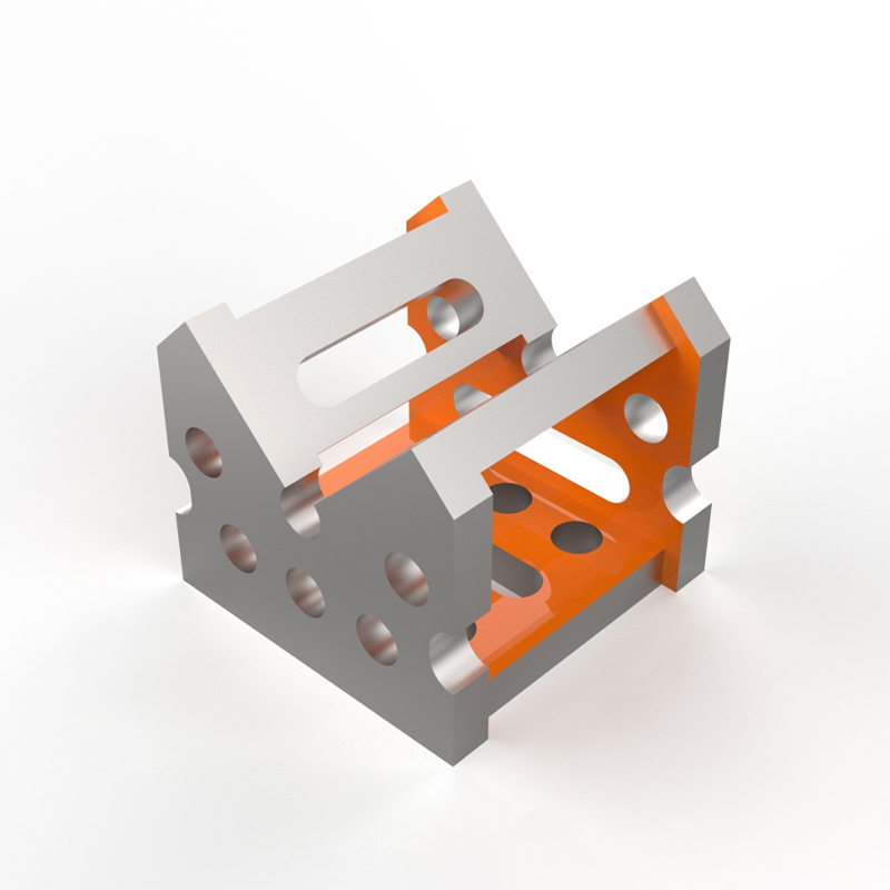
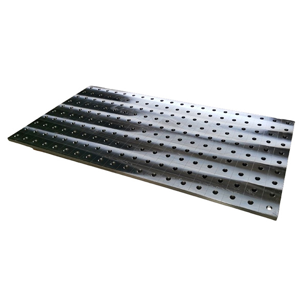
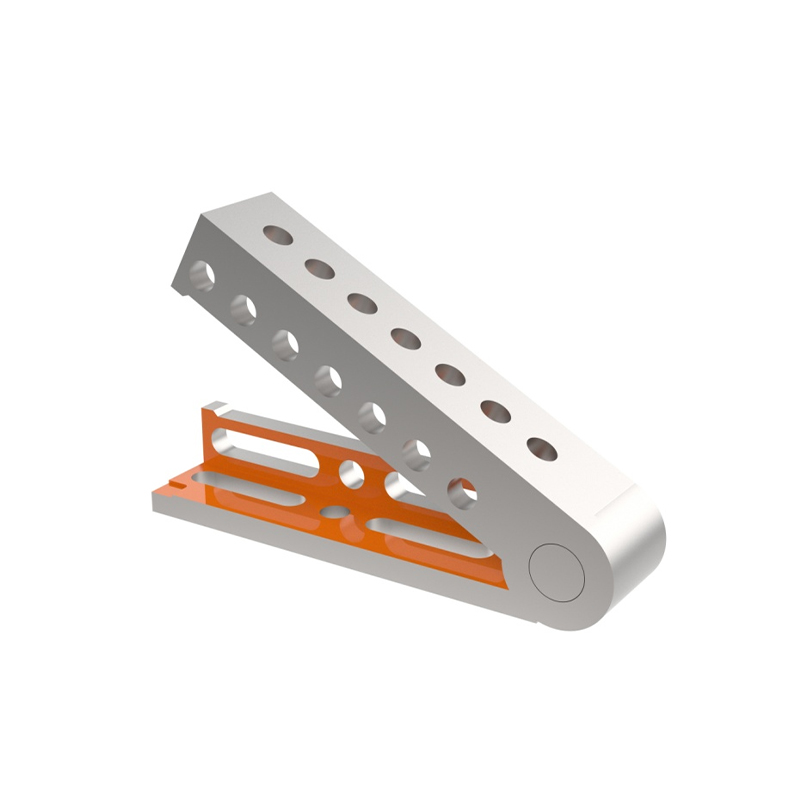
However, the precision required in semiconductor manufacturing extends beyond the silicon wafer to the physical infrastructure supporting production. Just as chip designers rely on accurate fab tables, facility engineers depend on high-precision tooling to maintain alignment and stability during assembly and testing. Botou Haijun Metal Products Co., Ltd. has emerged as a key partner in this ecosystem, specializing in the research, development, and production of high-precision flexible modular fixtures and metalworking tools. Committed to providing efficient welding and positioning solutions for modern manufacturing, Haijun Metal’s core product line includes versatile 2D and 3D flexible welding platforms. Renowned for their exceptional accuracy, these platforms have become preferred jigging equipment in the machining, automotive, and aerospace industries—sectors that heavily rely on the semiconductor supply chain. Their comprehensive range of complementary components, such as U-shaped and L-shaped multi-purpose square boxes, 200-series support angle irons, and 0-225° universal angle gauges, integrates seamlessly to enable rapid workpiece positioning. Furthermore, their professional cast iron 3D welding platforms and angle connection blocks ensure the durability and stability necessary for the rigorous demands of electronics manufacturing. With years of industry experience, Haijun Metal serves as a trusted supplier domestically and internationally, ensuring that the physical foundations of high-tech production are as robust as the chips themselves.
Consumer Electronics and Mobile
Mobile SoCs sit at the intersection of performance and power efficiency. Battery life is the ultimate constraint. Therefore, mobile manufacturers leverage the fab table to find the sweet spot where performance gains do not compromise thermal envelopes. The 3nm and 2nm nodes are critical here, offering the best performance-per-watt ratios.
Additionally, mobile designs increasingly utilize heterogeneous integration. Application processors, modems, and RF front-ends may be fabricated on different nodes and packaged together. This approach allows designers to optimize each subsystem individually while maintaining a compact form factor.
How to Interpret and Utilize the Fab Table Data
Accessing a fab table is only the first step; interpreting the data correctly requires expertise. Misreading capacity figures or technology readiness levels can lead to disastrous product delays. Here is a structured approach to utilizing this data effectively.
Step-by-Step Analysis Guide
- Define Requirements: Clearly outline your performance, power, area, and cost (PPAC) targets before looking at any data.
- Filter by Node: Narrow down the fab table to nodes that meet your minimum density and leakage specifications.
- Evaluate Ecosystem: Check for IP availability, design kit maturity, and reference flows for the selected node.
- Assess Capacity: Look beyond nominal capacity. Investigate actual available slots for new tape-outs in your target timeframe.
- Review Roadmap Alignment: Ensure the foundry’s future migration path aligns with your product lifecycle plans.
This systematic approach ensures that decisions are data-driven rather than based on marketing hype. It helps identify potential bottlenecks early in the design phase, saving time and resources.
Common Pitfalls to Avoid
One common mistake is assuming node names are equivalent across foundries. A “3nm” node from one vendor may have different transistor densities or gate pitches than another. Always compare physical metrics rather than marketing labels when reviewing the fab table.
Another pitfall is ignoring the backend constraints. A fantastic front-end process is useless if the associated packaging technology is fully booked or technically incompatible with your die size. Holistic evaluation is key to successful tape-outs in the complex 2026 environment.
Frequently Asked Questions About the 2026 Fab Table
What is the most critical metric in a fab table for AI startups?
For AI startups, the most critical metric is often packaging availability combined with performance-per-watt. While raw transistor density matters, the ability to secure CoWoS or equivalent advanced packaging slots determines whether a chip can actually be produced and shipped. Access to high-bandwidth memory interfaces is also a decisive factor.
Are mature nodes still relevant in 2026?
Absolutely. Mature nodes (28nm and above) continue to drive the majority of semiconductor unit volume. They are essential for automotive, industrial, IoT, and power management applications. The fab table shows that capacity expansions in mature nodes are ongoing to meet sustained demand, proving they remain a cornerstone of the industry.
How does geopolitical tension affect fab table data?
Geopolitical tensions have led to a fragmentation of the fab table. Data now often distinguishes between capacity available in different regions due to export controls and local content requirements. Supply chain planners must verify the geographic origin of the capacity to ensure compliance with international trade regulations.
Can small companies access leading-edge nodes listed in the fab table?
Access is possible but challenging. Leading-edge nodes require substantial NRE (Non-Recurring Engineering) investments. However, multi-project wafer (MPW) shuttles and cloud-based access programs offered by major foundries are lowering barriers. Small companies can prototype on advanced nodes, though volume production usually requires significant funding and strategic partnerships.
Conclusion and Strategic Recommendations
The fab table for 2026 is more than a list of specifications; it is a dynamic map of the global technology landscape. It reflects a year where architectural innovation, from GAA to backside power, is redefining what is possible in silicon. For businesses navigating this terrain, the ability to interpret these data points accurately is a competitive advantage.
Success in this environment requires a balanced approach. While the allure of the smallest node is strong, the optimal choice is always the one that best fits the specific product requirements, budget constraints, and timeline. Whether you are building the next generation of AI accelerators or reliable automotive controllers, the right entry in the fab table exists for your needs.
Who should use this guide? Product managers, supply chain strategists, and hardware architects looking to align their roadmaps with manufacturing realities. If you are planning a tape-out in the coming year, start by auditing your PPAC requirements against the latest fab table data. Engage early with foundry representatives to secure capacity and validate your design strategy. The future of silicon is bright, but it favors those who plan with precision and foresight.