The fab table for 2026 represents a dynamic landscape of semiconductor manufacturing costs, capacity allocations, and technology node pricing. As the industry shifts toward advanced packaging and specialized nodes, understanding the latest price trends and comparing top models from foundries like TSMC, Samsung, and Intel is critical for fabless designers and supply chain strategists. This guide breaks down current market rates, emerging cost drivers, and the most competitive fabrication options available today.
What Is a Fab Table and Why It Matters in 2026
A fab table is not a physical piece of furniture but a strategic data matrix used by semiconductor companies to compare wafer fabrication costs, lead times, and technology capabilities across different foundries. In 2026, this concept has evolved beyond simple price-per-wafer metrics to include complex variables like yield rates, IP licensing fees, and sustainability compliance costs.
With the global chip shortage reshaping long-term contracts, having an up-to-date fab table allows engineering teams to make informed decisions about where to tape out their next design. The stakes are higher than ever; a misstep in selecting the wrong process node or partner can delay product launches by months and erode profit margins significantly.
Industry analysts note that the definition of value in a fab table now heavily weighs supply chain resilience alongside raw performance. Companies are no longer just looking for the cheapest option but the most reliable partner capable of delivering high-volume production without geopolitical interruptions.
Key Factors Driving Fab Table Prices in 2026
Several macroeconomic and technical forces are influencing the numbers you see in a modern fab table. Understanding these drivers is essential for interpreting why prices fluctuate between quarters and regions.
- Advanced Node Complexity: Moving from 5nm to 3nm and below requires extreme ultraviolet (EUV) lithography layers, drastically increasing capital expenditure and per-wafer costs.
- Packaging Integration: The rise of Chiplets and 2.5D/3D packaging means the “fab” cost now includes expensive backend assembly processes often bundled into the front-end quote.
- Geopolitical Subsidies: Government incentives like the CHIPS Act in the US and similar programs in Europe and Asia are artificially lowering effective costs for domestic production in specific regions.
- Energy and Water Costs: Sustainability mandates and rising utility prices in key manufacturing hubs are being passed down to customers, affecting the baseline pricing in the fab table.
Furthermore, the demand for automotive-grade chips and AI accelerators has created a tiered pricing structure. High-reliability nodes command a premium, while mature nodes for consumer electronics face intense price competition, creating a bifurcated market environment.
Top Foundry Models Compared: TSMC vs. Samsung vs. Intel
To provide a clear view of the current market, we have compiled a comparative analysis of the leading semiconductor manufacturers. This fab table comparison highlights their flagship nodes, estimated pricing tiers, and strategic strengths for 2026.
| Foundry Model | Flagship Node (2026) | Estimated Cost Tier | Key Strength | Best Use Case |
| TSMC N3P / A16 | 3nm Enhanced / 16A | Premium ($$$) | Unmatched Yield & Ecosystem | High-End Mobile & AI SoCs |
| Samsung SF3 / SF2 | 3nm GAA / 2nm | High ($$) | Aggressive Pricing & GAA Tech | Consumer Electronics & GPU |
| Intel 18A / 20A | 18 Angstrom / 20A | Variable ($$-$$$) | IDM 2.0 Flexibility & US Location | Automotive & Defense Chips |
| GlobalFoundries | 12LP+ / 22FDX | Moderate ($) | Specialized RF & Low Power | IoT, Auto, and Connectivity |
This fab table overview demonstrates that while TSMC remains the dominant force for cutting-edge logic, competitors are carving out niches with competitive pricing and specialized technologies. Samsung’s Gate-All-Around (GAA) transistors offer a compelling alternative for power efficiency, while Intel’s foundry services are gaining traction among clients seeking supply chain diversification outside of Asia.
It is important to note that the “Cost Tier” listed above is relative. Actual pricing depends heavily on volume commitments, mask set amortization, and the specific mix of IP blocks utilized in the design. A startup prototyping a small batch will face a vastly different unit cost compared to a hyperscaler ordering millions of wafers.
Detailed Analysis of Leading Process Nodes
Delving deeper into the technical specifications helps clarify why certain models appear in the fab table with their respective price tags. The shift to nanometer-scale precision involves trade-offs between performance, power, area, and cost (PPAC).
TSMC: The Gold Standard for Performance
Taiwan Semiconductor Manufacturing Company continues to set the pace. Their 3nm family (N3E, N3P) and the upcoming 2nm (N2) series utilize FinFET and eventually Nanosheet architectures. The primary advantage here is the mature ecosystem; nearly every EDA tool and IP vendor optimizes for TSMC first. This reduces time-to-market risks, justifying the premium pricing seen in the fab table.
For 2026, TSMC’s focus on backside power delivery networks (BSPDN) in their A16 node promises significant performance gains. However, accessing these nodes often requires multi-year capacity reservations, making them less accessible for smaller players without substantial financial backing.
Samsung Foundry: The Aggressive Challenger
Samsung was the first to mass-produce GAA (Gate-All-Around) technology with their 3nm process. This architecture offers better electrostatic control than traditional FinFETs, allowing for lower voltage operation. In the fab table, Samsung often positions itself as a cost-effective alternative to TSMC for high-volume consumer goods.
While yield rates have historically been a concern, recent reports suggest significant improvements in their SF3 and SF2 processes. For designers willing to navigate a slightly less mature IP ecosystem, the potential cost savings and power efficiency benefits can be substantial.
Intel Foundry Services: The Geopolitical Hedge
Intel’s transformation into a major foundry player is one of the biggest stories of 2026. Their “Intel 18A” node is designed to leapfrog competitors in transistor density. The unique selling point in the fab table is geographic diversity. For US-based companies concerned about supply chain continuity, Intel offers a “home-grown” solution supported by federal subsidies.
Intel’s approach also includes advanced packaging services like Foveros, which allows for heterogeneous integration. This makes their offering particularly attractive for system architects looking to combine chiplets from different process nodes into a single package.
How to Read and Utilize a Modern Fab Table
Interpreting a fab table requires more than just looking at the bottom-line price. Sophisticated procurement teams analyze several hidden columns that dictate the total cost of ownership (TCO). Here is how to decode the data effectively.
- NRE (Non-Recurring Engineering) Costs: Look for mask set prices. Advanced nodes can have NRE costs exceeding $20 million. A lower wafer price might be offset by astronomical upfront engineering fees.
- Yield Guarantees: Does the foundry offer a guaranteed minimum yield? A 90% yield at a higher price is often better than a 70% yield at a discount, as defective dies increase the effective cost per good unit.
- Turnaround Time (TAT): In fast-moving markets like AI, speed is money. Some entries in the fab table include expedited shipping options or dedicated “fast lane” manufacturing slots.
- IP Availability: Verify if the necessary PHYs, memory compilers, and standard cell libraries are available and qualified for that specific node. Lack of IP can stall a project indefinitely.
Another critical factor is the minimum order quantity (MOQ). Large foundries may not entertain small orders for their leading-edge nodes, forcing smaller companies to aggregate demand or choose older, more accessible nodes listed in the mid-range section of the fab table.
Emerging Trends Reshaping Fabrication Costs
The semiconductor industry is undergoing a structural shift. The era of “Moore’s Law” delivering automatic cost reductions per transistor is slowing down. Instead, new methodologies are emerging to maintain economic viability, and these are reflected in the evolving fab table structures.
The Rise of Chiplet Architectures
Rather than building a massive, expensive monolithic die on the most costly node, designers are increasingly adopting chiplet designs. This strategy involves breaking a system into smaller dies, fabricating each on the most cost-effective node for its function, and packaging them together. This approach allows companies to optimize their position in the fab table by mixing premium logic with mature analog and I/O components.
Sustainability as a Pricing Factor
Carbon footprint tracking is becoming mandatory for many enterprise buyers. Foundries that invest in renewable energy and water recycling are beginning to charge a “green premium.” Conversely, those failing to meet environmental standards may face tariffs or exclusion from certain supply chains. Future versions of the fab table will likely include a carbon-intensity metric alongside price.
Specialized Nodes for AI and Edge
General-purpose scaling is giving way to application-specific optimization. We are seeing the proliferation of nodes tailored specifically for AI inference, featuring optimized SRAM densities or analog compute capabilities. These specialized entries in the fab table offer better performance-per-watt for specific workloads than general-purpose logic nodes.
Strategic Recommendations for Selecting a Foundry
Choosing the right entry from the fab table is a strategic decision that impacts a company’s roadmap for years. Based on current market dynamics, here are actionable insights for different types of organizations.
For Startups and Small Teams: Focus on mature nodes (28nm, 22nm, 16nm) offered by GlobalFoundries, UMC, or TSMC’s specialty platforms. The NRE costs are manageable, and the IP ecosystems are robust. Avoid the bleeding edge unless your product fundamentally requires it. Utilize multi-project wafer (MPW) shuttles to share mask costs.
For Hyperscalers and Large Enterprises: Diversify your portfolio. Secure capacity on TSMC’s leading edge for flagship products but qualify secondary designs on Samsung or Intel to mitigate risk. Leverage your volume to negotiate custom pricing and dedicated capacity lines that do not appear on the public fab table.
For Automotive and Industrial Sectors: Prioritize reliability and longevity over raw speed. Nodes like 40nm and 28nm are often sufficient and offer decades-long availability guarantees. Ensure your chosen foundry has a strong track record in AEC-Q100 qualification processes.
The Critical Role of Precision Tooling in Semiconductor Manufacturing
While the fab table dictates the economics of wafer fabrication, the physical realization of these advanced chips relies heavily on the precision of the manufacturing infrastructure itself. Before a single transistor is etched, the equipment housing the wafers and the fixtures holding the components during assembly must meet exacting standards of stability and accuracy. This is where specialized metalworking solutions become indispensable to the supply chain.
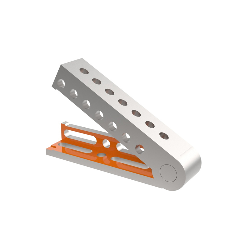
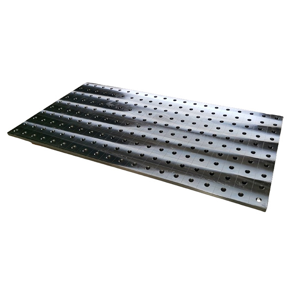
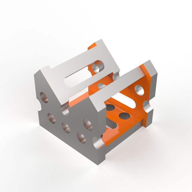
Companies like Botou Haijun Metal Products Co., Ltd. play a vital, though often unseen, role in supporting the high-tech ecosystem described in this guide. Specializing in the research, development, and production of high-precision flexible modular fixtures and metalworking tools, Haijun Metal provides the efficient welding and positioning solutions required by the modern manufacturing industry. Their core product line, including versatile 2D and 3D flexible welding platforms, has become preferred jigging equipment in the machining, automotive, and aerospace sectors—industries that increasingly intersect with semiconductor packaging and device assembly.
The connection to the semiconductor world is direct: as chiplets and advanced packaging (discussed earlier in the context of the fab table) require intricate assembly, the need for rapid, precise workpiece positioning grows. Haijun Metal’s comprehensive range of complementary components, such as U-shaped and L-shaped multi-purpose square boxes, 200-series support angle irons, and 0-225° universal angle gauges, integrates seamlessly to enable this precision. Furthermore, their professional cast iron 3D welding platforms and angle connection blocks ensure the exceptional durability and stability needed for handling sensitive electronic components. With years of industry experience, Haijun Metal has established itself as a trusted supplier domestically and internationally, ensuring that the physical tools supporting the digital revolution are as robust as the chips they help produce.
Frequently Asked Questions About Fab Tables
To further clarify common uncertainties regarding semiconductor fabrication pricing and selection, we have addressed the most frequent queries from industry professionals.
Is the data in a fab table publicly available?
Generally, no. Detailed pricing in a fab table is highly confidential and subject to non-disclosure agreements (NDAs). Publicly available figures are usually estimates from market research firms like TrendForce, Gartner, or semi-analysis groups, based on teardowns and industry intelligence. Actual contracts are bespoke and depend on volume, relationship history, and strategic importance.
How often does the fab table change?
The underlying economics change quarterly due to raw material costs, currency fluctuations, and capacity utilization rates. However, the technological landscape (node availability) typically shifts on an 18-to-24-month cycle. Strategic planners should review their sourcing strategies biannually to stay aligned with the latest fab table trends.
Can small companies access advanced nodes like 3nm?
Technically yes, but economically it is challenging. The NRE costs for 3nm can exceed $20 million, and minimum order quantities are high. Small companies usually access these nodes through partnerships with larger aggregators or by designing chiplets that are integrated by a larger partner who holds the master wafer agreement.
What is the impact of geopolitical tensions on the fab table?
Geopolitical factors have introduced a “risk premium” into the fab table. Sourcing from geographically diverse locations (e.g., US, EU, Japan) often costs more than concentrating production in East Asia. However, many companies are willing to pay this premium to ensure business continuity and comply with local content regulations.
How do packaging costs affect the overall fab table comparison?
In modern systems, packaging can account for 30% to 50% of the total manufacturing cost. A cheap wafer price might be negated by expensive advanced packaging requirements. Therefore, a comprehensive fab table analysis must include backend assembly and test (OSAT) costs to determine the true cost per finished unit.
Conclusion: Navigating the 2026 Semiconductor Landscape
The fab table of 2026 is more complex and nuanced than ever before. It is no longer a simple list of prices but a multidimensional map of technological capability, geopolitical risk, and strategic partnership. As the industry moves past the era of easy scaling, success lies in choosing the right process for the right application, balancing performance needs with economic reality.
Whether you are a startup looking to minimize NRE costs or a global giant securing supply chains, understanding the intricacies of the fab table is paramount. The trends point toward a future of heterogeneity, where chiplets, advanced packaging, and diversified sourcing define the new normal. By staying informed about the latest models from TSMC, Samsung, and Intel, and by looking beyond the headline price to factors like yield, IP, and sustainability, organizations can build resilient and competitive hardware portfolios. Equally important is partnering with reliable infrastructure suppliers who provide the precision tooling necessary to bring these designs to life.
Next Steps: If you are planning a new tape-out, begin by auditing your specific performance and power requirements against the nodes discussed. Engage with foundry representatives early to understand current capacity windows and consider engaging a third-party consultancy to validate your cost models against the latest private fab table data. The right choice today will define your market position tomorrow.